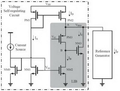
Fig. 1 Principle of voltage reference based on novel technique of self regulating of voltage
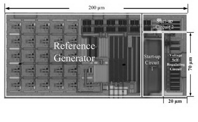
Fig. 2 Photo of chip

Fig. 3 Test results of high power supply rejection ratio of reference source
The Annual IEEE-CICC (Custom Integrated Circuits Conference) was recently held in San Jose, California. The CICC is one of the most important meetings in the IC design field. It has been held once a year since the beginning of 1988, and the contents of the conference have included integrated circuit design, simulation, production, MEMS, and biological electronics. The programmable chip and systematic research team of the Electronics Institute have recently made breakthroughs in the design technique of the inhibition of high power on ratio voltage reference, and the research study “A -115dB PSRR CMOS Bandgap Reference With a Novel Voltage Self-Regulating Technique” was reported at the conference, as one of the rare conference reports with mainland China units as the main author.
Voltage reference voltage source is a very important module in high-speed mixed number model chips, and the stability of the reference voltage directly affects the performance of the entire system. Facing the complicated noise environment in the mixed system, the reference source must have a high power supply rejection ratio in order to provide a stable voltage reference for the high-speed mixed signal chip. In the traditional design of high power supply rejection ratio of reference sources, an LDO (low power differential linear voltage-stable apparatus) was used to provide the reference source with local stable power source, in order to improve the power inhibition ratio of the reference source. Although this approach is simple and practical, it requires the use of an additional operational amplifier which has a high power consumption and occupies a large area. However, with the rise of wearable devices and mobile devices, SoC systems have become more complex. Greater numbers of high-speed digital circuits, RF circuits, switched capacitors and circuits are integrated on the same silicon chip. Analog circuits not only need to face more interference of high-frequency noise, but are also require to be more stringent on power consumption and area, which gives rise to a novel challenge for the design of reference source circuits: how to achieve a high power supply rejection ratio of large band width ranges under the circumstance of low power consumption and small area.
In view of the above difficulties, this paper proposes a novel type of self-regulating technique, which achieved a reference source (high power supply rejection ratio) without the use of a filter capacitor, LDO or operational amplifier. The novel self-regulating circuit was used to provide a reference source with local power, which effectively improved the low/high frequency power supply rejection ratio of the reference source under the circumstance of low energy consumption and small area.
The principle figure of voltage reference based on the novel self-regulating technique is shown in Fig. 1. The self-regulating technique first converts the voltage fluctuation of the power supply to the current, then it arrives at the ground by the low resistance branch bypass (as shown in the shaded part of Fig. 1), thus resulting in a clean local power. The technique abandoned the traditional LDO method, thereby greatly saving power consumption and area, and causing a significant inhibitory effect on power supply noise. The self-stabilization technique can also be used for improving the power inhibition ratio of other power supply noise sensitive circuits such as comparators, operational amplifiers, etc.
The entire circuit used the CMOS craft design with a standard of 0.18 µm, and the chip photo is illustrated in Fig. 2. The measurement results of the reference source power supply rejection ratio are shown in Fig. 3. The power supply rejection ratio at low frequency is up to -115 dB and at 10 MHz is up to -90 dB, thus the test results are superior to those described in similar studies.
(11th Department, Tao Yin)